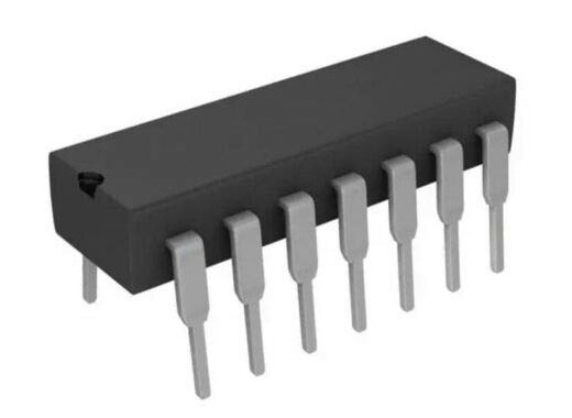
One component that finds ubiquitous use in circuits is the 74LS08. This versatile chip, part of the 74 series integrated circuits family, is widely employed in various applications, from simple logic gates to complex digital systems. In this article, we will explore the functionalities and applications of the 74LS08 quad 2-input AND gate, shedding light on its importance in the world of digital electronics.
Overview of the 74LS08 Quad 2-input AND Gate
The 74LS08 is an integrated circuit (IC) that contains four independent 2-input AND gates. It is commonly used in digital logic circuits to perform logical operations such as conjunctions. The chip’s compact design and low power consumption make it an ideal choice for a variety of applications, ranging from simple hobby projects to complex industrial machinery.
Texas Instruments and the 74LS08

Texas Instruments is one of the leading companies involved in the production of the 74LS08 IC. The company has been producing high-quality electronic components for decades, and their expertise in the field makes them a reliable source for these types of products. The 74LS08 is just one example of the many quality ICs that Texas Instruments offers, making it a great choice for those seeking dependable and efficient electronic components.
Other notable ICs from Texas Instruments worth exploring
In addition to the 74LS08, Texas Instruments has a wide range of other notable ICs that are worth exploring. Some examples include the LM386 audio amplifier, the LM317 voltage regulator, and the TPS series of power management ICs. These components are often used in various electronics applications and have proven to be highly reliable and efficient.
74LS08 Datasheet and Pinout
The 74LS08 datasheet provides detailed technical information on the chip’s electrical and mechanical characteristics. This information is critical when designing circuits that incorporate the 74LS08 IC. The datasheet contains information on the chip’s supply voltage, input voltage, output voltage, and output current, among other specifications. Understanding these specifications is essential in designing circuits that function reliably and efficiently.
The 74LS08 pinout is a diagram that illustrates the physical arrangement of the chip’s pins and their corresponding functions. The pinout is essential when wiring the chip into a circuit, as it indicates the correct orientation and connection of each pin. Each pin serves a unique function, such as VCC, GND, input, and output pins. Understanding the functionality of each pin is important in designing circuits that function correctly and accurately.
Tips for Using 74LS08 Effectively
To use the 74LS08 effectively, it is essential to follow certain best practices for circuit design and layout considerations. One key aspect is to ensure proper power supply decoupling by placing decoupling capacitors near the VCC and GND pins of the IC. This helps to reduce noise and maintain stable power delivery. Additionally, it is recommended to minimize long trace lengths between the IC and external components to minimize signal degradation and improve overall performance.
Signal integrity is another crucial consideration when using the 74LS08. To maintain optimal performance, it is critical to minimize signal reflections and ensure clean, well-defined input signals. This can be achieved by using termination resistors or impedance matching techniques when necessary. Careful attention should also be given to routing sensitive signals away from noise sources and providing suitable ground planes to minimize interference.
Troubleshooting common issues and potential solutions when using the 74LS08
When encountering issues with the 74LS08, it is helpful to be familiar with common troubleshooting techniques.
- One common issue is incorrect wiring or connections, so verifying the pinout and cross-checking connections can help identify and resolve such problems.
- Additionally, issues related to power supply voltage levels, such as insufficient voltage or excessive fluctuations, can affect the performance of the IC. Using appropriate power supply regulation and monitoring techniques can help address these issues and improve the reliability of the circuit.
Comparison to Other Similar ICs

There are alternative quad 2-input AND gate ICs available, such as the 74HC08 and the CD4081. While these ICs perform similar functions, they may have differences in terms of electrical characteristics, power consumption, speed, and compatibility. The 74LS08 is known for its low power consumption and high-speed operation, making it suitable for applications with tight power constraints and where fast response times are required.
When considering the advantages and disadvantages of the 74LS08 in relation to its competitors, it is important to evaluate specific application requirements. The 74LS08 excels in low-power applications and can operate at high speeds, but it may not be the best choice for applications that require a wide supply voltage range or compatibility with different logic families.
Factors such as cost, availability, and ease of integration within the existing system should also be considered when choosing the ideal IC for a project. It is recommended to thoroughly review datasheets and application notes from different manufacturers to make an informed decision.
Conclusion
74LS08 is a versatile and essential component in the realm of digital electronics. Its ability to perform logical AND operations on multiple inputs makes it an invaluable tool in designing robust and efficient digital circuits. This integrated circuit finds widespread use in a myriad of applications, from basic logic gate implementations to intricate digital systems.


